Trigger
Delay trigger circuit
Early the circuit was originally designed as analogue
delay device for trigger signals. With sufficient short adjusted
delay times it can be used to manipulate sync signals, too. It is
based on the standard logic IC 74HC123 »dual retriggerable
monostable multivibrator with reset«. Of course, a digital
timer with micro-controller (poss. commercial kit) is more precise,
but so simple and versatile as well? (Some day there will come a
suitable app for sure, if it doesn't exist already. ;-)
Just an addition to trigger points and delay times: in TTL
technology a level above 2.2 V is interpreted as HIGH and a
level below 0.8 V as LOW. Switching times - and given delay
times - can use this scheme, but need not. Thus there is e.g. the
10% to 90% way - below 10% of full level LOW and above 90% of full level
HIGH, resp. - or 50% - half full level - as start points. And there
are even current loop controlled devices like PLCs ...
Delay trigger

Phase shifter (delay trigger)
Basic function
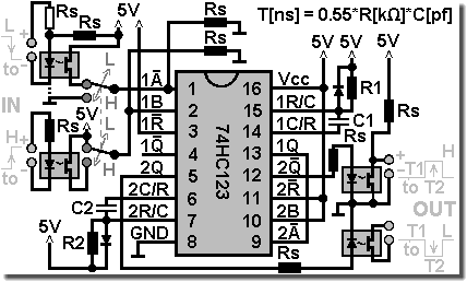
A pulse at the input interface is released at the output delayed with T1 =
k x R1 x C1 and lasting T2 = k x R2 x C2. T2 lengthen a short pulse
enabling reaction of the device to be controlled. With sufficient
short T1 + T2 the circuit can be used as delay device for sync
signals as well.
Typical values: R1, R2 = 0.2 to 1 MOhm; C1, C2 = 0 to
several µF; Rs = 1 kOhm at the diodes of the opto couplers,
some 10 kOhm at the inputs 1|A and 1B. Possibly one has to
select the shunt resistors at the input IN L to fit to the
trigger/sync voltage and perhaps one has to bridge the white
outlined one. (Factor k is depending of the IC family and the
manufacturer. Its value is about 0.35 to 0.65. In the figure it is 0.55.)
Additional functions
Some extensions are integrated in the circuit: at the output OUT H a control signal with rising edge is always available and OUT L always offers one with falling edge (exact short circuit). Thus one can convert an input signal. Only one input channel, however, can be used at a time, IN L with short circuit or falling edge signals and IN H with rising edge signals. The unused input of the 74HC123 must be set to a certain potential, 1|A to GND and 1B to +5 V. Therefore a double (coupled) switch is designed in. If one exclusively uses one input, the other one can be soldered to the certain potential making the switch not necessary.
Connections
The opto couplers provide protection for the 74HC123. One,
however, can feed in the signals directly, but then one should put
the device into a socket to ease exchange. The most secure and preferred
path is IN H to OUT L, because it is potential free. Suitable opto
couplers at the input (shunt resistor in the diode branch!) offer
the possibility to work with signal sources different from
5 V, e.g. at a PLC with 24 V.
The resistors Rs are used for current limitation reasons or as
drain path in switching processes. The diodes parallel to R1 and R2
are used to discharge large C1 and C2 after (fast) power down and
protect the 74HC123.
Supply
One can gain the +5 V e.g. inside the PC from the old four pole floppy or harddisk drive power connector (white housing; red cable = +5 V, black cable = GND) or from a suitable interface connector (USB ...).
Additional options
Selecting potentiometers instead of the certain resistors R1 and
R2 offers the variable adjusting of delay times.
Setting the reset inputs 1|R and 2|R not permanently to +5 V but
with switching capability from GND to +5 V one gets a trigger
enable feature, e.g. for safety reasons. Not before these inputs are
switched to +5 V the IC is active and waits for the valid input
signal.
The inputs could be extended by Schmitt triggers to do signal
conditioning. And some status LEDs would complete the device.
Trigger device

Low ohms path in the trigger device
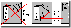
Especially some additional words about triggering with
falling etch: the system to be triggered usually awaits a fast
voltage drop caused by the trigger source, thus some kind of short
circuit. (Even it would be done with a paper clip.) Connecting a
battery and then simply de-plug the wires will not work usually. A
low ohm path is really necessary, e.g. a closing switch,
while the battery is not really requires, because the system
provides the voltage of the trigger input all alone.
One can measure this voltage, e.g. +5 V in case of
common TTL level, with a multi-meter, because its high internal
resistance does not release the trigger.
The reverse equivalent is valid for triggering with rising edge -
with removing the short circuit the voltage of the trigger input
rises and releases the trigger.
Special cases
Synchronous trigger
Eventually it can pay to synchronize the trigger signal
to the system clock. For instance by holding the trigger pulse in a
flip flop (e.g. a D-Latch), using its output pins anded (AND gate)
with the system clock as valid trigger signal further on.
Thereby one avoids that the trigger signal shows a variable
trigger offset within the associated frame. With the delay device
mentioned above this value can even be adjusted.
Propagation delay
Eventual delays due to limited spreading speeds of signals can usually be ignored. A rule of thumb - the speed of signals in wires is about 2/3 to full speed of light, thus about 0.2 to 0.3 m (2/3 to 1 feet) in a nanosecond or 200 to 300 m (about 650 to 1000 feet) in a microsecond due to signal slopes being slurred by e.g. capacitive loads and inductivities of the cables. (Rule of thumb: light, and therefore electromagnetic waves like current, travels with one foot, 30 cm, per nano second. Even gate delays of electronic devices lie within this region, too.)

